Field Note
ASU AEP Solar Fab Tour
- Photovoltaic fabrication
- Materials and processes
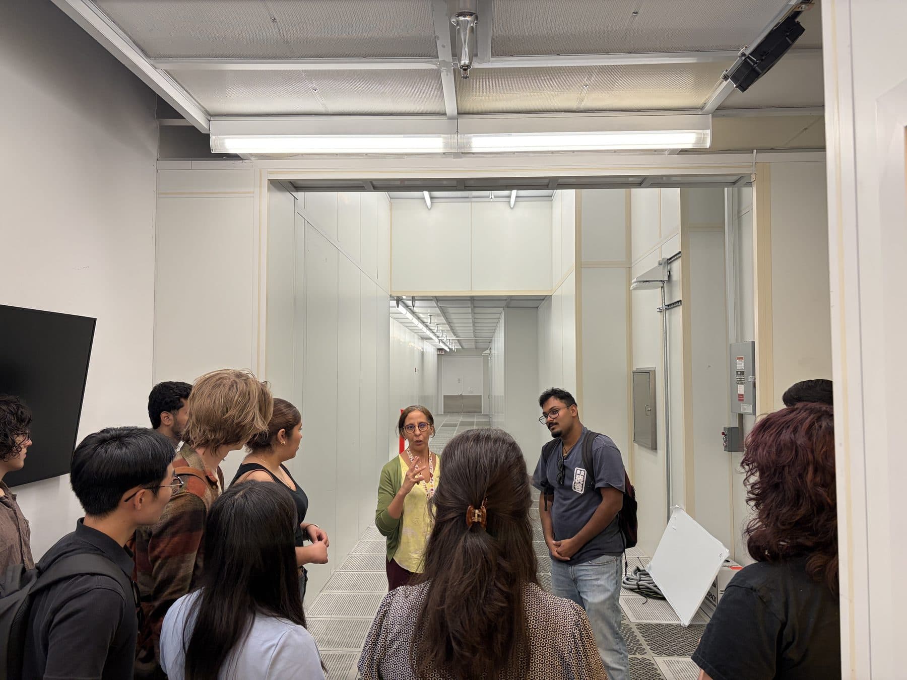
A behind-the-scenes tour of the ASU AEP Solar Fab led by Wardia Debray, Process Engineer, following how photovoltaic devices move through fabrication and the materials and processes behind solar technology.
What the visit made visible
Three observations from the chapter’s event record and photographs.
Start with the material
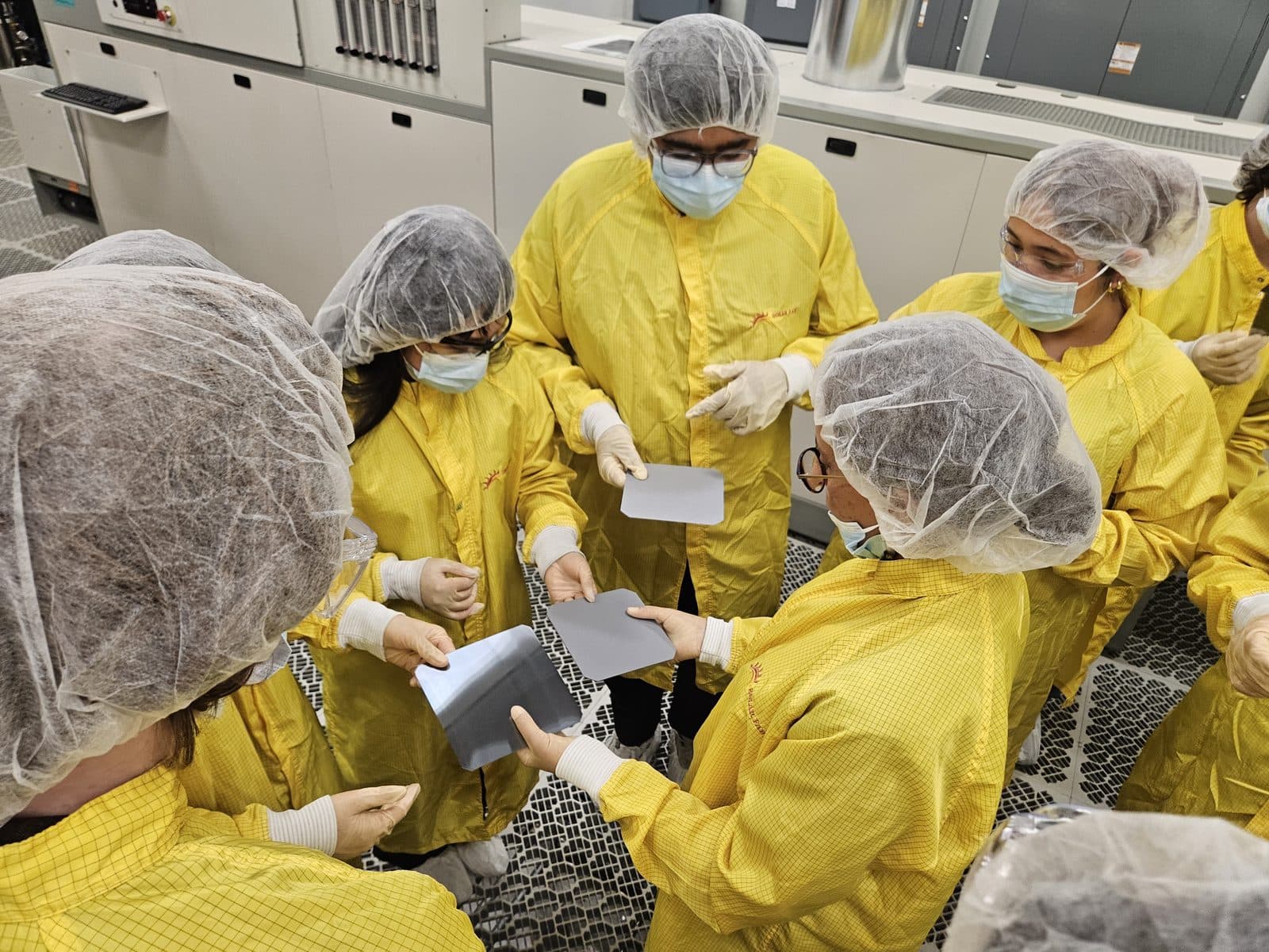
Students examined thin samples up close. The photograph records a moment of handling and comparison, alongside the tour’s broader focus on the materials and processes behind photovoltaic devices.
Look beyond a single device
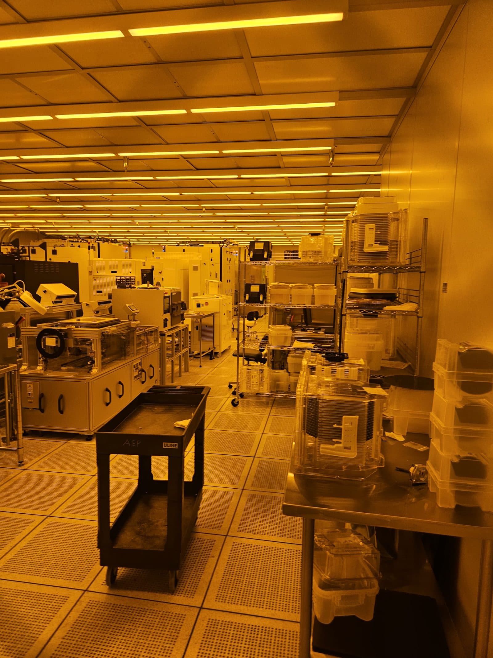
The facility photographs show process equipment, storage and work areas throughout the fabrication space. The visit followed how photovoltaic devices move through fabrication, connecting the device to the environment in which it is made.
Notice how people enter the process
Students wore cleanroom gowns, hair covers, face masks and gloves inside the facility. Those details are visible alongside the samples and tools: the working environment includes people and procedures as well as equipment.
Inside the visit